Kioxia 10th-Gen BiCS FLASH NAND Targets AI Data Centers
**Keywords:** Kioxia, BiCS FLASH, 3D NAND, AI data centers, Kitakami fab, enterprise SSD, METI subsidies, TLC NAND, Yokkaichi plant, Japan semiconductor, hyperscaler demand, 10th-gen NAND, SK Hynix, Micron Sample Shipment Details Kioxia Holdings Corp. announced the start of sampling for its 10th-generation BiCS FLASH on July 3, 2026, according to reports in the Japan Times. The
Sample Shipment Details
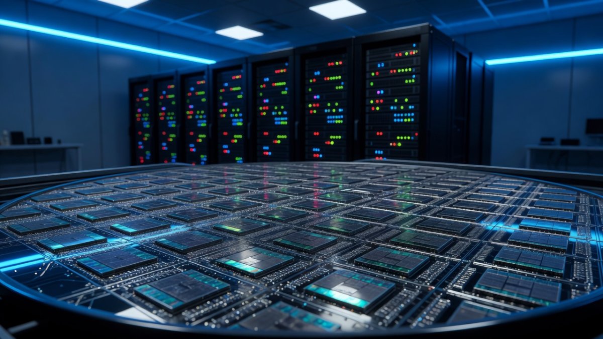
Kioxia Holdings Corp. announced the start of sampling for its 10th-generation BiCS FLASH on July 3, 2026, according to reports in the Japan Times. The company shipped initial samples of the 1Tb TLC 3D NAND devices to select partners focused on AI infrastructure. These shipments mark the first external validation of the new generation outside Kioxia's internal testing facilities. The recipients include leading hyperscale operators and enterprise storage developers who require immediate evaluation for upcoming server platforms. This measured release allows Kioxia to gather performance data under real AI training workloads before wider distribution.
(Global 1 News)
The sampling process emphasizes higher efficiency and faster data transmission characteristics tailored specifically for AI data center environments. Engineers at Kioxia prepared the samples with optimized firmware that highlights power savings during sustained read and write cycles. Partners receiving the devices are expected to conduct extensive qualification tests over the coming months. Such testing will verify compatibility with existing controller architectures used in large-scale storage arrays. The July 3 milestone reflects years of process development at Kioxia's Japanese fabrication sites.
Tokyo-based Kioxia coordinated the announcement through its corporate communications channels to underscore Japan's ongoing role in advanced memory technology. The sampled devices represent the culmination of iterative improvements following the company's 2018 separation from Toshiba. Early recipients have already begun integrating the NAND into prototype SSDs designed for large language model training clusters. Feedback from these initial deployments will directly influence final design tweaks ahead of volume production. This deliberate approach minimizes risks associated with introducing new memory generations into mission-critical AI systems.
Industry observers note that the timing of the July 3 sampling aligns with rising capital expenditure by hyperscalers on storage infrastructure. Kioxia limited the initial shipment quantities to maintain quality control during the evaluation phase. The company continues to supply reference designs and technical documentation alongside the physical samples. These supporting materials help customers accelerate their own system-level validation efforts. Overall, the shipment details demonstrate Kioxia's strategic focus on high-value AI segments rather than broad consumer markets.
Technical Specifications and Architecture
The 10th-generation BiCS FLASH features a 1Tb TLC configuration built on advanced 3D stacking technology. This architecture increases bit density while preserving the reliability required for continuous AI data center operation. Kioxia engineers achieved these gains through refined vertical channel formation and improved charge trap layer materials. The resulting device delivers enhanced power efficiency compared with previous generations during intensive parallel access patterns. Interface speeds have also been elevated to support the rapid data movement demanded by large language model training.
Compared with the 9th-generation product, the new NAND reduces energy consumption per bit transferred through optimized peripheral circuitry. The 3D stacking height has been increased without compromising yield, allowing more layers within the same package footprint. This structural evolution directly addresses the thermal constraints found in densely populated AI server racks. Faster toggle-mode interfaces enable quicker handoff between the NAND dies and the SSD controller. Such improvements collectively position the 10th generation as a meaningful step forward in storage performance per watt.
Triple-level cell operation remains central to the design, balancing cost-effective density with the endurance levels needed for enterprise workloads. Kioxia incorporated additional error-correction enhancements at the array level to maintain data integrity over extended periods. Power efficiency metrics show particular strength during idle states, which is critical when thousands of drives sit in large storage pools. The architecture also supports higher sustained write bandwidth, reducing bottlenecks during dataset ingestion for model training. These specifications reflect careful tuning for the unique access profiles of AI applications.
Thermal management features have been integrated into the die layout to handle the heat generated by high-speed interfaces. Kioxia validated the design across multiple temperature ranges typical of data center environments. The combination of increased layer count and refined process geometry yields a meaningful capacity increase per chip. This density improvement helps system designers reduce the total number of packages required for a given storage target. Overall, the technical foundation supports both current AI needs and anticipated future scaling requirements.
Competitive Landscape
Samsung Electronics continues to lead in overall NAND market share with its own high-layer 3D products aimed at similar AI applications. Micron Technology has introduced competing high-density TLC solutions that emphasize cost-per-bit advantages in hyperscale deployments. SK Hynix maintains a strong position through close collaboration with major memory controller vendors and server OEMs. Each competitor pursues incremental layer count increases as part of the ongoing race to deliver greater areal density. Kioxia differentiates itself through its focus on power efficiency metrics particularly valued by Japanese and European data center operators.
The layer count race remains intense, with all major players pushing beyond 200 layers in their latest roadmaps. Kioxia's 10th-generation device enters this environment with a balanced approach that prioritizes transmission speed alongside density. Samsung's offerings often target broader consumer and mobile segments in addition to enterprise use. Micron has accelerated qualification cycles for its latest nodes to capture share in North American hyperscale accounts. SK Hynix benefits from vertical integration within its broader semiconductor portfolio, enabling tighter system-level optimization.
Kioxia's positioning centers on reliability and long-term supply stability for customers concerned about geopolitical concentration risks. The company leverages its heritage in NAND development to offer customized firmware solutions for AI-specific command sets. While competitors may announce higher headline capacities, Kioxia emphasizes measured improvements in sustained performance under heavy AI workloads. This strategy appeals to operators planning multi-year infrastructure investments rather than short-term capacity spikes. Market analysts expect continued fragmentation as each vendor carves distinct niches within the enterprise SSD segment.
Price competition remains fierce, yet Kioxia avoids pure commodity positioning by highlighting total cost of ownership benefits from lower power draw. The enterprise SSD segment is projected to outgrow consumer NAND markets, intensifying rivalry among the four major suppliers. Kioxia must demonstrate consistent yield improvements to remain cost-competitive at scale. Partnerships with Japanese equipment makers provide some insulation from global supply chain volatility. The competitive dynamics will ultimately be shaped by which vendor best matches the evolving performance envelope of next-generation AI accelerators.

(Global 1 News)
Japan's Semiconductor Revival Strategy
The Japanese government has designated semiconductors a strategic priority under its economic security framework. METI provides targeted subsidies to support domestic production capacity and technology development at companies such as Kioxia. These measures aim to reduce reliance on overseas manufacturing for critical memory components used in AI infrastructure. Kioxia, spun off from Toshiba in 2018, has become a focal point for these national efforts to rebuild advanced semiconductor capabilities. The subsidies help offset the substantial capital requirements of next-generation NAND process nodes.
The Kitakami fab in Iwate prefecture serves as the primary site for ramping the 10th-generation BiCS FLASH. Government funding has supported cleanroom expansions and equipment installations necessary for the new process. Yokkaichi plant in Mie prefecture continues as the company's primary manufacturing base, handling both legacy and advanced production lines. This dual-site strategy provides operational resilience while concentrating cutting-edge development at Kitakami. METI's involvement ensures alignment with broader goals of supply chain security for digital infrastructure.
Post-Toshiba history has seen Kioxia navigate complex ownership structures while maintaining technological leadership in 3D NAND. The separation allowed focused investment in memory-specific research without competing corporate priorities. National subsidies now accelerate the transition from sampling to mass production, shortening the timeline compared with purely commercial funding models. Policymakers view successful execution at Kioxia as a bellwether for Japan's ability to compete in high-value semiconductor segments. Collaboration between industry and government extends to workforce development programs that address specialized engineering talent needs.
Economic security considerations also influence export control policies and international partnership frameworks. Kioxia benefits from stable domestic energy and infrastructure support that complements the METI funding. The revival strategy emphasizes not only production volume but also intellectual property retention in critical process technologies. Continued government backing will be essential as global competition for AI-related memory capacity intensifies. These coordinated efforts position Japan to maintain a meaningful role in the future of data center storage.
AI Data Center Demand Drivers
Large language model training imposes unprecedented requirements on storage subsystems for rapid dataset access and checkpointing. High-density NAND solutions such as Kioxia's 10th-generation device directly address the capacity and bandwidth needs of these workloads. Hyperscalers are expanding enterprise SSD deployments to support distributed training clusters that span thousands of GPUs. The growth trajectory of the enterprise SSD segment is expected to significantly outpace traditional consumer NAND markets over the next several years. This shift creates sustained demand for power-efficient, high-performance memory components.
AI model parameter counts continue to scale, driving corresponding increases in training data volumes that must reside on fast local storage. Kioxia's emphasis on faster transmission speeds aligns with the need to minimize data movement latency between storage and compute nodes. Enterprise customers prioritize drives that maintain consistent performance across mixed read-write patterns typical of model iteration cycles. The resulting demand surge has prompted all major NAND suppliers to accelerate their AI-optimized roadmaps. Storage architects now design systems around the assumption of continuous high-utilization AI workloads.
Hyperscale operators evaluate total cost of ownership metrics that heavily weight power consumption and cooling requirements. Devices offering superior efficiency per terabyte delivered gain preference in large-scale procurement decisions. Kioxia's 10th-generation architecture targets exactly these parameters through refined 3D stacking and interface improvements. The enterprise SSD market expansion also reflects broader digital transformation initiatives beyond pure AI research. Yet AI training remains the most visible catalyst for near-term capacity additions in data centers worldwide.
Supply chain planning at major cloud providers now incorporates multi-year forecasts tied to AI roadmap announcements from chip designers. This forward visibility benefits memory manufacturers capable of committing to volume production timelines. Kioxia's sampling phase provides early signals that the company intends to participate actively in this growing segment. Demand drivers extend beyond training to include inference serving and retrieval-augmented generation systems that also require substantial persistent storage. The interplay between AI compute scaling and storage density improvements will shape industry investment patterns for the remainder of the decade.
Production Timeline and Market Outlook
Kioxia has targeted 2027 for mass production of the 10th-generation BiCS FLASH at the Kitakami fab. This schedule allows sufficient time for customer qualification cycles following the July 3, 2026 sampling start. Qualification involves rigorous endurance, retention, and performance testing under simulated AI data center conditions. The company must demonstrate stable yields at the new process node before committing to high-volume output. Government support through METI subsidies helps underwrite the capital expenditures required during this ramp phase.
Yield challenges inherent to increased layer counts will require ongoing process optimization throughout 2026 and into 2027. Kioxia draws on its experience at the Yokkaichi plant to transfer lessons learned from prior generations to the Kitakami line. Early production volumes will likely be allocated to strategic customers who participated in the sampling program. This measured approach reduces the risk of quality issues reaching the broader market. Market outlook remains positive given the structural growth in enterprise SSD demand driven by AI adoption.
Customer qualification timelines typically span nine to twelve months, placing initial revenue recognition in the latter half of 2027. Kioxia continues to invest in test equipment and failure analysis capabilities to accelerate this phase. Broader market adoption will depend on competitive pricing relative to Samsung, Micron, and SK Hynix offerings. The enterprise SSD segment's projected outperformance versus consumer markets provides a favorable demand backdrop. Sustained government backing for domestic semiconductor production further strengthens the long-term outlook for Kioxia's advanced NAND roadmap.
Global supply dynamics suggest that successful execution of the 2027 mass production target could secure meaningful share gains for Kioxia in the AI storage segment. Potential delays from equipment lead times or process integration issues remain key risks to monitor. The company maintains parallel development of subsequent generations to ensure continuity beyond the 10th-generation node. Overall, the combination of technical capability, national strategic support, and aligned market demand positions Kioxia for a significant role in the evolving AI data center ecosystem through the end of the decade.
Tags: Kioxia, BiCS FLASH, 3D NAND, AI data centers, Kitakami fab, enterprise SSD, METI subsidies
By Kenji Tanaka, Staff Writer
What's Your Reaction?
 Like
0
Like
0
 Dislike
0
Dislike
0
 Love
0
Love
0
 Funny
0
Funny
0
 Wow
0
Wow
0
 Sad
0
Sad
0
 Angry
0
Angry
0
Japan Correspondent at Global1.News. Tokyo-based voice covering Japanese politics, technology, economy, and culture. Tracks the intersection of tradition and innovation in one of the world's most dynamic societies.


Comments (0)