
Tower Semiconductor's $3B Japan Bet on Silicon Photonics
In a bold play to secure Japan's foothold in the exploding AI infrastructure market, Tower Semiconductor's massive commitment to silicon photonics could shift the balance of power in optical connectivity away from traditional players in Taiwan and the United States.
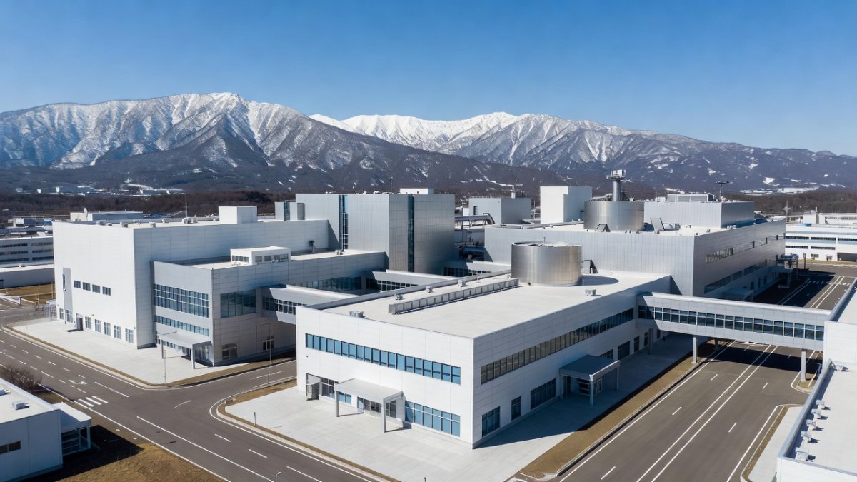
In a bold play to secure Japan's foothold in the exploding AI infrastructure market, Tower Semiconductor's massive commitment to silicon photonics could shift the balance of power in optical connectivity away from traditional players in Taiwan and the United States. By leveraging decades-old Japanese fabs and fresh government backing, the company aims to deliver the high-bandwidth, low-power links that hyperscale data centers desperately need. This expansion signals a new chapter in specialty semiconductors where light, not just electrons, drives the next wave of computing performance.
Tower Semiconductor's $3 Billion Japan Bet Reshapes Silicon Photonics
Tokyo, Japan – July 22, 2026 — Article continues...
Announcement Details and Investment Structure
Tower Semiconductor announced on July 14, 2026 a $3 billion dual-track expansion across existing and new sites in Japan. The Israeli foundry, listed as TSEM on NASDAQ and TASE, will receive approximately $1 billion in grants from the Ministry of Economy, Trade and Industry. Track one involves repurposing the Arai facility, formerly TPSCo Fab 6, to install 300mm silicon photonics capacity together with advanced packaging lines. Track two calls for construction of an additional 300mm wafer fab next to the existing Fab 7 in Uozu, Toyama Prefecture, to raise overall output of both silicon photonics and silicon germanium devices.
The Arai and Uozu sites trace their roots to TPSCo’s origins as former Panasonic Semiconductor operations. Both locations in Toyama Prefecture have maintained 300mm wafer processing expertise for more than two decades, giving Tower immediate access to qualified clean-room infrastructure and process engineers already familiar with high-volume specialty manufacturing.
Panasonic Semiconductor, founded in the 1970s, built its reputation on discrete devices and analog ICs before spinning off its fabs into the TPSCo joint venture in 2011 with Tower. This long industrial lineage left behind not only physical infrastructure but also proprietary process recipes for high-voltage and RF technologies that now accelerate silicon photonics development.
This heritage reduces the typical ramp-up risks associated with new photonics lines. Existing metrology and etch tools at Arai can be upgraded rather than replaced outright, allowing Tower to accelerate qualification of silicon photonics modulators and germanium photodetectors while preserving institutional knowledge built during the Panasonic era.
Timeline and Production Readiness
Production readiness at the repurposed Arai site is expected in the fourth quarter of 2027. The new Uozu facility will follow a phased schedule that aligns with demand growth for optical components in artificial intelligence clusters. These dates remain subject to equipment qualification and regulatory approvals, consistent with the measured pace of prior Japanese semiconductor projects.
Equipment lead times for specialized photonics tools such as deep-UV lithography and wafer-level testing systems remain a key variable. Suppliers have quoted 12-to-18-month delivery windows for 300mm-compatible modules, which could compress the qualification window if METI grant milestones are strictly enforced.
Talent competition with Rapidus and TSMC Kumamoto adds further scheduling pressure. Tower must attract experienced process and device engineers in a market where these three projects are simultaneously recruiting from the same limited pool of Japanese and expatriate specialists.
Strategic Alignment with National Semiconductor Policy
The investment forms part of Japan’s broader semiconductor renaissance. In fiscal year 2026 the government has allocated roughly ¥1.23 trillion, equivalent to $8.2 billion, for semiconductor manufacturing and artificial intelligence infrastructure. METI selected Tower to lead capacity growth in silicon photonics and silicon germanium, technologies viewed as critical for next-generation data movement. Tower has maintained operations in Japan since acquiring a majority stake in the former Panasonic Semiconductor facilities, now operated as TPSCo, giving the company established process know-how and a trained workforce.
Japan’s cumulative public and private semiconductor commitments since 2021 now surpass $42 billion when Rapidus’s multi-year Hokkaido program and TSMC’s Kumamoto investments are included. This sustained funding dwarfs earlier decades of incremental support and reflects Tokyo’s determination to rebuild domestic resilience after years of foundry capacity migration overseas.
Japan’s Semiconductor and Digital Industry Strategy deliberately emphasizes specialty technologies rather than leading-edge logic nodes. Unlike the U.S. CHIPS Act ($52 billion) or the EU Chips Act ($47 billion), METI funding prioritizes materials, analog, and photonic capabilities that complement rather than compete with global foundry leaders.
The “Clean Room” strategy coordinated by METI further supports this approach by subsidizing shared infrastructure that multiple specialty players can access, lowering individual capital barriers while accelerating collective technology adoption across the domestic supply chain.
Support for AI Data Center Optical Connectivity
Silicon photonics enables higher bandwidth and lower power optical links inside and between AI servers. Tower’s expanded 300mm lines will address rising demand from hyperscale operators that require dense, cost-effective optical engines. Silicon germanium processes complement these efforts by supporting high-speed analog and radio-frequency components used in optical transceivers. The company has stated that the projects directly target this AI-driven connectivity market.
Silicon photonics integrates waveguides, modulators, and detectors directly onto silicon wafers using CMOS-compatible steps, enabling monolithic co-integration with electronic circuits. In contrast, silicon germanium excels in carrier mobility for high-frequency amplification and low-noise transimpedance amplifiers but offers no native optical functionality, making the two technologies complementary rather than competitive within the same transceiver module.
Bandwidth requirements are scaling rapidly from 400G to 800G and 1.6T per port. Silicon photonics on 300mm wafers offers the only economically viable path to integrate hundreds of optical channels per package while maintaining the power efficiency that copper interconnects can no longer achieve at these data rates.
Co-packaged optics (CPO) architectures further amplify the advantage. By placing photonic engines directly beside switch ASICs, CPO reduces electrical trace lengths and associated power losses, a critical factor as AI cluster power consumption approaches tens of megawatts per rack row.
Revenue and Profitability Targets
Tower has set corporate goals of $3.6 billion in revenue and $1.2 billion in net profit for 2028. Achievement depends on successful ramp of the new Japanese capacity, continued utilization at existing global sites, and sustained customer demand for specialty silicon processes. Chief Executive Officer Russell Ellwanger noted the government’s selection of Tower to lead expansion of these strategically important technologies.
Positioning Within Asia-Pacific Technology Competition
Japan’s support for Tower occurs alongside other large-scale projects. Rapidus is advancing a $34 billion state-backed effort in Hokkaido focused on leading-edge logic. TSMC is investing approximately $17 billion in Kumamoto for 3-nanometer production. Tower’s focus on specialty technologies such as silicon photonics and silicon germanium occupies a distinct segment that complements rather than duplicates these logic-centric initiatives. The combination strengthens Japan’s position relative to foundry capacity in Taiwan and South Korea while addressing supply-chain resilience concerns involving China.
China’s silicon photonics push through SMIC and Loongson seeks to localize optical components for domestic AI accelerators. TSMC’s COUPE platform and South Korea’s HBM-plus-optical-interconnect programs add further competitive pressure, making secure, diversified supply chains for photonic engines a geopolitical priority for Japan and its allies.
Contribution to Society 5.0 Objectives
Japan’s Society 5.0 vision integrates cyber and physical systems to solve social challenges. Expanded domestic production of silicon photonics supports high-speed data infrastructure required for smart cities, autonomous mobility, and advanced medical imaging. By increasing local manufacturing of these components, the Tower project contributes to the data backbone that underpins Society 5.0 applications without relying solely on imported modules.
Technology Implications for Japanese Industry
Silicon photonics capacity at Arai and Uozu directly benefits Japanese optical component makers such as Fujitsu and Oki Electric. These firms can source high-performance silicon photonic integrated circuits locally rather than importing dies, shortening design cycles for next-generation optical transceivers and reducing exposure to export controls on advanced packaging equipment.
Data center operators in Japan gain access to lower-latency, power-efficient interconnects that support the dense GPU clusters required for domestic AI training. This capability strengthens the broader electronics supply chain by anchoring high-value photonic assembly and testing jobs inside Japan instead of allowing them to migrate to Taiwan or Southeast Asia.
Outlook and Remaining Considerations
Execution risks include equipment lead times, clean-room construction schedules, and qualification of new 300mm photonics processes. METI grants reduce capital burden but require milestone compliance. Tower’s long-standing presence through TPSCo provides operational continuity that may shorten learning curves compared with green-field entrants. The July 2026 announcement marks a concrete step in Japan’s effort to regain prominence in specialty semiconductor manufacturing while meeting global demand for optical connectivity in artificial intelligence systems.
KEPCO power availability for the expanded Toyama fabs and sustained access to specialized photonics process tools will determine whether the 2027–2028 ramp stays on schedule. Tower’s established TPSCo footprint offers a meaningful advantage in navigating these constraints relative to newer entrants.
By Kenji Tanaka, Staff Writer
This article was produced with AI-assisted research and editorial support. Reporting is based on sources cited in the article.
What's Your Reaction?
 Like
0
Like
0
 Dislike
0
Dislike
0
 Love
0
Love
0
 Funny
0
Funny
0
 Wow
0
Wow
0
 Sad
0
Sad
0
 Angry
0
Angry
0

Japan Correspondent at Global1.News. Tokyo-based voice covering Japanese politics, technology, economy, and culture. Tracks the intersection of tradition and innovation in one of the world's most dynamic societies.













Comments (0)