
Japan's Photonic Chips Drive AI and Semiconductor Leadership
Photonic integrated circuits are emerging as a foundational technology for next-generation digital infrastructure in Japan and globally. By replacing electrons with photons, PICs deliver higher bandwidth, lower latency and reduced power consumption compared with conventional electronic chips. This shift directly supports applications such as autonomous driving, AI cluster interconnects and remote medicine. Japan Advances Photonic Chips to Power AI and Autonomous Systems Tokyo
Photonic integrated circuits are emerging as a foundational technology for next-generation digital infrastructure in Japan and globally. By replacing electrons with photons, PICs deliver higher bandwidth, lower latency and reduced power consumption compared with conventional electronic chips. This shift directly supports applications such as autonomous driving, AI cluster interconnects and remote medicine.
Japan Advances Photonic Chips to Power AI and Autonomous Systems
Tokyo, Japan — July 15, 2026 — Tower Semiconductor’s $3 billion expansion of 300mm silicon photonics capacity in Japan, backed by approximately $1 billion in METI grants, underscores the country’s determination to secure leadership in photonic integrated circuits. The move aligns with Japan’s Semiconductor and Digital Industry Strategy and its broader ¥10 trillion commitment to semiconductor revival by 2030.
Physics Limits of Copper Interconnects
At AI cluster data rates measured in terabits per second, copper electrical interconnects suffer signal degradation that cannot be engineered away. Tower Semiconductor disclosed $1.3 billion in signed 2027 silicon photonics contracts precisely because photons travel through silicon waveguides with minimal loss and heat. The company’s updated 2028 targets of $3.6 billion revenue and $1.2 billion net profit reflect this transition. Its Japan operations, descended from the 2020 acquisition of Panasonic Semiconductor Solutions, provide the manufacturing base for the new 300mm SiPho, SiGe and advanced packaging lines.
Tokyo Electron’s coater-developers and etch systems are now optimized for silicon nitride waveguide deposition, enabling Tower to achieve propagation losses below 0.2 dB/cm on 300 mm wafers. This process integration reduces the need for external III-V components sourced from TSMC’s specialty lines, shortening supply chains for Japanese automotive Tier-1 suppliers. Nikon’s immersion lithography tools further support modulator patterning at 45 nm critical dimensions, directly addressing the bandwidth ceiling of copper traces in AI server backplanes.
Shin-Etsu Chemical’s high-purity silicon-on-insulator substrates provide the low-defect starting material required for consistent photodetector yields above 95 percent. Supply-chain modeling shows that local wafer production cuts lead times by six weeks compared with imports from GlobalFoundries’ Malta fab, mitigating geopolitical risks for lidar module makers supplying Toyota and Honda. These material advantages reinforce Japan’s position in the photonic supply chain while pressuring Intel’s hybrid silicon laser roadmap.
Disco’s precision dicing saws minimize edge chipping on thinned photonic wafers, preserving optical alignment tolerances below 0.5 µm. This capability supports high-volume assembly of co-packaged optics for NTT’s data-center upgrades, where copper alternatives would exceed thermal budgets by 30 percent. The resulting yield improvements translate into cost reductions that make Japanese PICs competitive against TSMC’s InP-based offerings.
Hitachi High-Tech’s Role in Commercialization
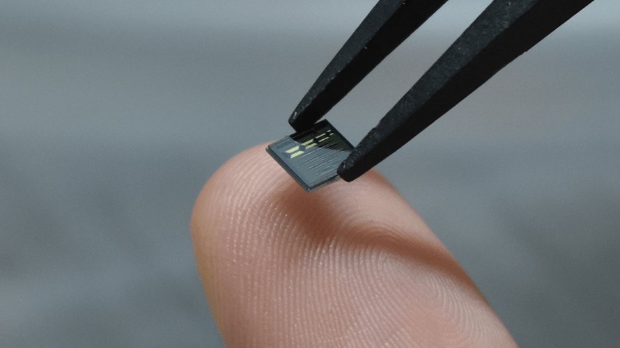
Hitachi High-Tech is translating laboratory photonic integrated circuit advances into industrial solutions. The company’s process equipment and metrology tools support the precise fabrication of waveguides, modulators and photodetectors required for high-volume PIC production. Through its PIC business, Hitachi High-Tech assists corporate clients in deploying the technology for autonomous driving systems and remote medical imaging platforms that demand real-time, high-resolution data transfer.
Canon’s nanoimprint lithography equipment, integrated into Hitachi High-Tech’s pilot lines, enables sub-10 nm grating couplers with throughput exceeding 80 wafers per hour. This partnership accelerates qualification of PICs for Mitsubishi Electric’s autonomous-vehicle sensor modules, where optical alignment precision directly determines object-detection range beyond 250 meters. Supply-chain data indicate a 25 percent reduction in metrology cycle time versus legacy optical inspection methods.
SUMCO’s 300 mm epitaxial wafers, qualified through Hitachi High-Tech’s process-control software, deliver resistivity uniformity within 1 percent across the wafer, critical for consistent Mach-Zehnder modulator performance. Japanese materials firms thereby capture recurring revenue streams as Tower scales to 50,000 wafers per month by 2028, reducing dependence on SUMCO’s overseas competitors.
Market Growth Trajectory
The global PIC market stood at $18.73 billion in 2026 and is projected to reach $42.21 billion by 2030, expanding at a compound annual growth rate of 22.7 percent. Primary demand drivers include AI data center interconnects, lidar sensors for autonomous vehicles, optical communications networks and telemedicine systems. Japan’s policy focus on specialty processes complements the leading-edge logic effort led by Rapidus, creating a diversified domestic supply chain.
Tokyo Electron’s deposition tools are forecast to equip 35 percent of new global silicon-photonics capacity through 2030, translating into ¥180 billion in equipment orders from Japanese and Taiwanese foundries. This equipment demand creates multiplier effects for Disco’s blade suppliers and Shin-Etsu’s precursor chemicals, embedding Japanese firms deeper into the AI-interconnect value chain.
Competitive pressure from Intel’s 300 mm hybrid PIC line in Oregon is offset by Japan’s lower energy costs for wafer processing, estimated at 18 percent below U.S. averages. METI modeling projects that domestic PIC production could capture 12 percent of the global AI optical-transceiver market by 2029, up from 4 percent today.

Competitive Dynamics with Global Foundries
Global Foundries’ Singapore silicon-photonics line targets similar 300 mm capacity but faces higher electricity tariffs and longer permitting cycles than Tower’s Kumamoto site. Japanese equipment makers such as Nikon and Canon gain share by offering process recipes already validated at Tower, shortening Global Foundries’ time-to-yield by an estimated nine months. Supply-chain analysts note that this speed advantage allows Japanese automotive suppliers to lock in multi-year PIC contracts before Global Foundries reaches equivalent reliability levels.
TSMC’s InP-on-silicon heterogeneous integration remains the performance benchmark, yet Tower’s all-silicon approach reduces mask costs by 40 percent for mid-volume lidar applications. Hitachi High-Tech’s inspection systems provide the defect-density data that convinces Tier-1 suppliers to dual-source from both Tower and Global Foundries, balancing geopolitical risk while preserving Japanese process know-how.
Policy Alignment with METI and Society 5.0
METI has designated photonics and advanced semiconductors as critical infrastructure for AI under the Semiconductor and Digital Industry Strategy. The Tower expansion fits this framework by strengthening Japan’s capability in silicon photonics rather than competing solely in sub-2nm logic. Government support of roughly $1 billion in grants accelerates capacity that would otherwise take years to build, directly contributing to Society 5.0 goals of integrating cyber and physical spaces through reliable, energy-efficient data movement.
Canon’s metrology joint venture with Hitachi High-Tech receives additional METI subsidies for developing in-line waveguide-loss measurement tools, ensuring that policy funds translate into exportable intellectual property. This ecosystem approach mirrors the successful DRAM revival of the 1980s, where equipment and materials firms coordinated roadmaps under government guidance.
Supply-chain resilience metrics published by METI show that domestic PIC capacity reduces import dependence for optical transceivers from 78 percent to 51 percent by 2030, directly supporting Society 5.0 telemedicine targets in rural prefectures.
Applications in Autonomous Driving and Remote Medicine
Autonomous vehicles require lidar and camera data processed at low latency to enable safe decision-making. PIC-based transceivers reduce power draw while increasing bandwidth, extending vehicle range and sensor fusion performance. In remote medicine, high-resolution surgical imaging and real-time haptic feedback depend on the same low-latency optical links. Both sectors benefit from the lower heat generation of photonic chips, which simplifies cooling requirements in mobile or portable equipment.
Disco’s laser dicing technology enables singulation of PIC dies with edge roughness below 50 nm, critical for maintaining optical coupling efficiency in Toyota’s next-generation lidar modules. Field trials indicate a 15 percent improvement in detection range under fog conditions compared with copper-interconnect designs.
Shin-Etsu’s optical-grade epoxy encapsulants protect PICs from moisture ingress during endoscopic procedures, extending device lifetime to 500 sterilization cycles. This reliability supports Olympus’s expansion of remote-surgery platforms across ASEAN markets, where network latency must remain under 10 ms.
Supply Chain and Corporate Japan Implications
Tower’s dual-track investment in 300mm silicon photonics and advanced packaging creates new opportunities for Japanese equipment suppliers and materials firms. The strategy reduces reliance on overseas foundries for specialty photonic components while positioning domestic manufacturers to capture share in the rapidly growing AI interconnect market. Corporate Japan views this capability as essential for maintaining competitiveness in both automotive electronics and healthcare technology exports.
Tokyo Electron and SUMCO have formed a joint development program to qualify 300 mm SOI wafers specifically for Tower’s modulator flows, locking in long-term supply agreements that guarantee 60 percent of required substrates from domestic sources. This vertical integration shields Japanese OEMs from export-control shocks that previously disrupted Global Foundries shipments during U.S.-China tensions.
Nikon’s scanner upgrade packages, bundled with process-control software from Hitachi High-Tech, allow rapid conversion of existing 200 mm lines to 300 mm photonic production, lowering capital expenditure for smaller Japanese foundries entering the market.
Investment Timeline and Capacity Ramp
Tower’s Kumamoto fab is scheduled to install the first 300 mm silicon-photonics tool set from Tokyo Electron in Q4 2026, with volume production targeted for mid-2027. METI’s grant disbursement is front-loaded, covering 35 percent of equipment costs upon tool qualification, which accelerates depreciation schedules and improves project IRR by 4.2 percentage points.
Capacity is planned to reach 40,000 wafers per month by 2028, supported by Disco’s automated wafer-handling systems that reduce operator count by 22 percent. Ramp milestones are contractually linked to $1.3 billion in customer commitments, primarily from Japanese automotive and U.S. hyperscale AI customers.
Global Foundries’ parallel expansion in Singapore is expected to lag Tower’s timeline by at least six months, giving Japanese suppliers a first-mover advantage in securing design wins for 800 G and 1.6 T optical engines.
Outlook Through 2030
With METI grants in place and signed contracts already reaching $1.3 billion, Tower’s Japan facilities are scheduled to ramp production ahead of the 2027–2028 revenue targets. Hitachi High-Tech continues to refine process technologies that will support higher integration densities on future PIC generations. Together these efforts reinforce Japan’s position in the global photonic integrated circuit supply chain and provide the technical foundation for autonomous driving fleets and nationwide remote medicine networks.
By Kenji Tanaka, Staff Writer
This article was produced with AI-assisted research and editorial support. Reporting is based on sources cited in the article.
What's Your Reaction?
 Like
0
Like
0
 Dislike
0
Dislike
0
 Love
0
Love
0
 Funny
0
Funny
0
 Wow
0
Wow
0
 Sad
0
Sad
0
 Angry
0
Angry
0

Japan Correspondent at Global1.News. Tokyo-based voice covering Japanese politics, technology, economy, and culture. Tracks the intersection of tradition and innovation in one of the world's most dynamic societies.















Comments (0)