
India’s Semiconductor Journey: Old Designer, New Producer
India’s semiconductor trajectory, long celebrated for its design acumen, entered a new phase in September 2026 as the nation unveiled the second installment of its India Semiconductor Mission (ISM 2.0).
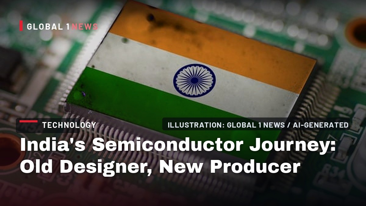
India’s semiconductor trajectory, long celebrated for its design acumen, entered a new phase in September 2026 as the nation unveiled the second installment of its India Semiconductor Mission (ISM 2.0). The policy shift, announced by Electronics and IT Minister Ashwini Vaishnaw, moves “from demonstrating intent to executing projects at scale,” positioning India as a trusted partner in the global chip value chain. This article examines the historical underpinnings of India’s chip industry, the strategic objectives of ISM 2.0, and the geopolitical currents that shape its prospects, drawing on recent observations from the fifth edition of SEMICON India.
Historical Foundations: From Early Ambitions to Design Dominance
India’s engagement with semiconductor manufacturing dates back to the 1980s, when a concerted push placed the country only a narrow margin behind the world’s most advanced process technologies. This early momentum was abruptly halted by a catastrophic fire in 1989 at the state‑run Semiconductor Complex Limited in Mohali, an event that crippled domestic fab capacity. The subsequent 1991 economic liberalization further eroded manufacturing zeal, as imported chips became cheaper and Indian fabs struggled with limited subsidies, bureaucratic hurdles, and inadequate infrastructure.
Despite the setback in fabrication, India cultivated a robust design ecosystem. Today, roughly one‑fifth of the world’s chip‑design talent operates out of Indian Global Capability Centers (GCCs) in Bengaluru, Hyderabad, Noida, and Pune, delivering research and development for multinational giants such as Intel, Qualcomm, Texas Instruments, and NXP. This design strength, rooted in a legacy of technical expertise, forms the intellectual backbone of the nation’s contemporary semiconductor strategy.
ISM 1.0: Early Wins and Persistent Gaps
The first phase of the India Semiconductor Mission, launched several years earlier, succeeded in approving twelve manufacturing projects, including nine packaging units and the construction of India’s inaugural commercial fab. These achievements demonstrated the government’s capacity to mobilize capital and attract private investment for fab development. Nonetheless, the sector remains heavily dependent on imports, with more than ninety percent of chip‑making equipment sourced from abroad, underscoring a critical supply‑chain vulnerability.
ISM 1.0’s focus on expanding physical fab capacity did not address the deeper structural deficiency: the scarcity of domestic semiconductor‑grade equipment, specialty chemicals, and gases. Without a homegrown supplier base, Indian fabs must continue to rely on foreign inputs, limiting the strategic autonomy that the mission ultimately seeks.
ISM 2.0: Funding, Ownership, and the Full‑Stack Vision
Approved in July 2026, ISM 2.0 is allocated an outlay of approximately $13 billion. The policy framework emphasizes two measurable strengths: the volume of intellectual property (IP) generated by Indian talent and the proportion of fab inputs sourced domestically. To bridge the ownership gap, the mission funds full‑stack Indian semiconductor IP, seed‑stage startups, and design incentives tied to deployment. Crucially, strategically important chip designs supported under ISM 2.0 are to be co‑owned by a state agency, ensuring that the resulting IP remains within national borders.
This co‑ownership clause, while intended to safeguard strategic assets, may complicate licensing, acquisition, and venture‑capital financing for fabless startups. The balance between state control and market‑driven growth will be a decisive factor in whether India’s design talent can be transformed into globally competitive, Indian‑owned enterprises.
Supply‑Chain Development: Building a Domestic Equipment Base
Beyond IP, ISM 2.0 allocates fiscal support to domestic producers of semiconductor equipment, chemicals, gases, and raw materials. The objective is to reduce the current reliance on imported tooling, which exceeds ninety percent, and to foster a self‑sustaining ecosystem akin to the pathways taken by Taiwan, South Korea, and Japan. Achieving this requires not only capital infusion but also the cultivation of tacit knowledge and long‑term supplier relationships, elements that historically emerge only through sustained state commitment over multiple funding cycles.
The mission’s success will hinge on the ability to attract and retain firms capable of delivering semiconductor‑grade equipment—a sector that demands high precision, deep technical expertise, and substantial upfront investment. Early indications suggest that global players, motivated by diversification away from Taiwan and China, are already committing resources to India, a trend that could accelerate the development of a domestic supply base.
Geoeconomic Context: De‑Risking and the Friend‑Shoring Paradigm
India’s semiconductor ambitions intersect with broader geopolitical dynamics. The United States, European Union, Japan, and South Korea are actively de‑risking their supply chains by reducing dependence on Taiwan and mitigating exposure to China. This strategic shift has spurred investments from companies such as Micron and Applied Materials in Indian fab projects, positioning India as a politically stable node within the global network.
Analysts have advocated for a trilateral chip cooperation among Japan, South Korea, and India, leveraging each nation’s comparative advantages—Japan’s equipment expertise, South Korea’s fabrication capacity, and India’s vast market and labor force. While the durability of this friend‑shoring model depends on the persistence of U.S.–China tensions, current assessments suggest that these frictions are unlikely to abate in the near term, thereby sustaining India’s attractiveness as a diversification destination.
Challenges Ahead: From Capital to Capability
The principal obstacle confronting ISM 2.0 extends beyond the allocation of subsidies. The mission must nurture a domestic ecosystem of semiconductor‑grade equipment manufacturers and specialty chemical suppliers, a process that historically required decades of incremental development in East Asian economies. Establishing such a base involves cultivating tacit knowledge, fostering iterative supplier relationships, and ensuring long‑term capital availability—conditions that cannot be satisfied by a single funding tranche.
Moreover, the policy’s IP co‑ownership requirement introduces a tension between state oversight and entrepreneurial agility. If licensing frameworks become overly cumbersome, they may deter venture capital and impede the scaling of fabless startups, thereby limiting the translation of design talent into indigenous chip enterprises.
Forward Outlook: Measuring Ownership and Input Localization
India’s semiconductor future will be judged by two interlinked metrics: the rise in Indian‑owned IP and the increase in domestically sourced fab inputs. Success in both dimensions would signify a genuine transition from an “old designer” to a “new producer,” aligning with the mission’s stated goal of moving from intent to execution at scale. Conversely, stagnation in either area could relegate India’s chip story to a peripheral role in the global supply chain, dependent on external de‑risking trends rather than intrinsic capability.
As the fifth SEMICON India exhibition concluded on 19 September, showcasing over 600 exhibitors and 300 international firms from 52 countries, the event underscored both the ambition and the complexity of India’s semiconductor ecosystem. The exhibition’s theme, “Silicon to Systems: Building the Ecosystem,” encapsulated the dual challenge of nurturing design excellence while constructing a resilient supply chain. In the months and years ahead, scholars and policymakers alike will watch closely whether ISM 2.0 can deliver on its promise, thereby reshaping the geopolitical and economic contours of the global semiconductor landscape.
This article was produced with AI-assisted research and editorial support. Reporting is based on the source material cited below. Sources: The Diplomat; thediplomat.com; Global1.News (28 September 2026).
By Prof. David Park, Staff Writer
What's Your Reaction?
 Like
0
Like
0
 Dislike
0
Dislike
0
 Love
0
Love
0
 Funny
0
Funny
0
 Wow
0
Wow
0
 Sad
0
Sad
0
 Angry
0
Angry
0

East Asia/Technology Correspondent at Global1.News. Seoul-based voice covering Korean politics, technology, business, and culture. Analyzes how technology and geopolitics intersect across East Asia.












Comments (0)