
Google Unveils TPU 8i Max and TPU 8tx: A Dual-Chip TPU and a Confidential TPU
Google just rolled out two new configurations for its eighth‑generation TPU family, and the hype train is already chugging full‑steam. Both are marketed as solutions for massive context windows and regulated workloads, respectively.
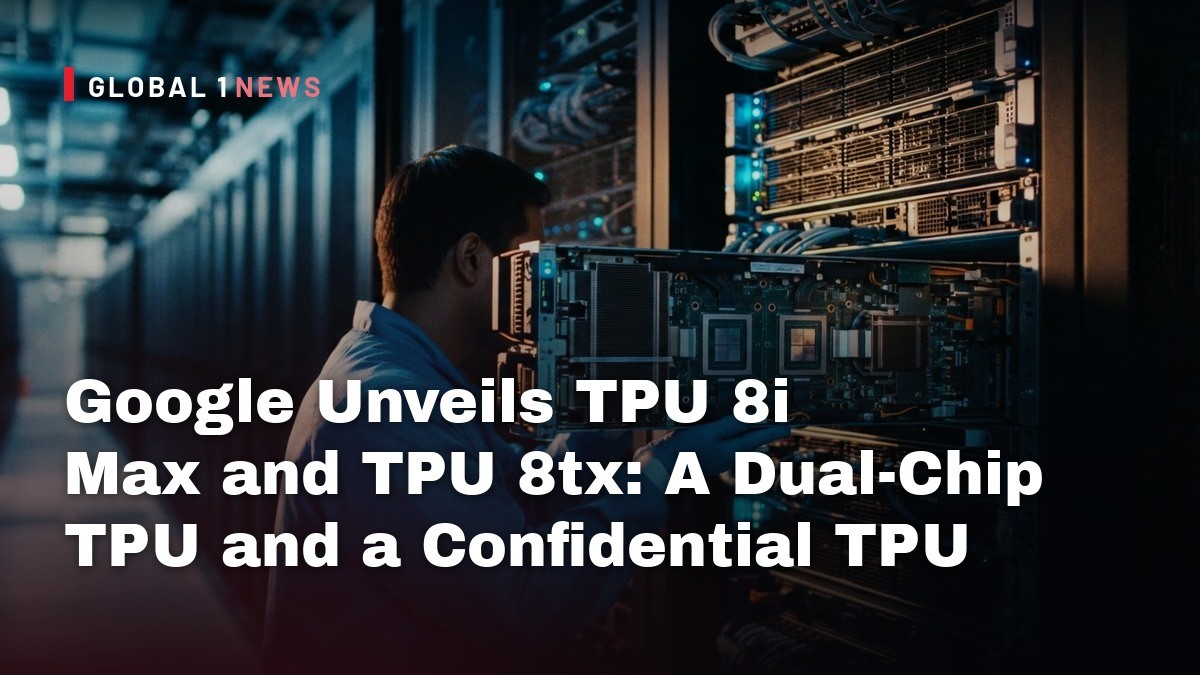
Google just rolled out two new configurations for its eighth‑generation TPU family, and the hype train is already chugging full‑steam. The TPU 8i Max is a dual‑chip package that doubles the compute, SRAM and HBM bandwidth of the existing TPU 8i, while the TPU 8tx is a “confidential inference” offering built on the same silicon as the TPU 8t but paired with 5th‑gen AMD EPYC hosts. Both are marketed as solutions for massive context windows and regulated workloads, respectively. As a founder who runs real hosting infrastructure day‑in, day‑out, I’m less interested in the marketing fluff and more in what these moves mean for independent cloud providers, the cost curve, and the real‑world risk profile of relying on Google’s ever‑shifting stack.
What Google actually shipped
The announcement makes it clear that Google isn’t unveiling a brand‑new chip; it’s re‑packaging existing eighth‑gen silicon. The TPU 8i Max simply places two low‑latency TPU 8i dies into a single package, effectively doubling the per‑chip figures that Google published for the 8i. Each 8i chip is rated at 10.1 PFLOPS of FP4, 288 GB of HBM and 8,601 GB/s of bandwidth, plus 384 MB of on‑chip SRAM. By stacking two of these, the Max configuration should deliver roughly 20.2 PFLOPS, 768 MB of SRAM and 17.2 TB/s of HBM bandwidth per package, although Google has not officially disclosed those absolute numbers.
The TPU 8tx, on the other hand, keeps the same TPU 8t silicon but couples it with 5th‑gen AMD EPYC CPUs and adopts the Boardfly network from the 8i line. Google claims up to a 2× latency reduction versus the standard TPU 8t, with “near‑zero” security penalty for confidential inference. The key selling point is that data and model weights stay encrypted even while the model is running, eliminating the need to move sensitive workloads between separate clusters.
Why the “dual‑chip” trick matters (or doesn’t)
From a hardware‑ops perspective, packing two dies into the same rack footprint is a clever way to squeeze more performance out of an existing design without a full silicon redesign. It means you get roughly double the compute density for the same power and cooling envelope that Google already supports. For hyperscalers, that’s a win – they can sell more FLOPS per rack without re‑tooling fabs. For independent providers, however, the benefit is murkier. Google’s pricing model for TPU services is opaque, and historically the cost per TFLOP has been higher than on‑prem GPUs when you factor in data egress and network charges.
In practice, the “twice‑the‑silicon” claim translates into a larger memory wall. The TPU 8i Max doubles the HBM bandwidth to about 17.2 TB/s, which is impressive on paper but also means the host system must be able to feed that bandwidth without bottlenecking. Smaller hosting outfits typically lack the ultra‑high‑speed interconnects (e.g., 400 Gbps Ethernet or custom silicon fabrics) that Google’s own data centers enjoy. The result is a classic case where advertised specs look great until you try to feed them with commodity networking and storage.
Confidential inference: hype or genuine advantage?
The TPU 8tx is pitched at regulated enterprises and governments that need to keep data encrypted even during inference. Google’s approach is to keep the model weights and input data encrypted in memory, only decrypting within the TPU’s secure enclave. This is a step up from the usual “decrypt‑in‑CPU‑memory‑then‑process” model, but the claim of “near‑zero” security penalty is largely marketing speak. In real deployments, you still have to trust the host CPU (the AMD EPYC) to manage keys and orchestrate the secure enclave, and you’re still dependent on Google’s software stack to enforce the isolation.
For an independent hosting provider, the biggest risk is vendor lock‑in. If your customers demand confidential inference, you’ll likely have to route them through Google Cloud’s TPU 8tx offering, which means you lose control over data residency and pricing. Moreover, the TPU 8tx does not come with disclosed performance numbers, so you can’t benchmark it against alternative confidential‑compute solutions (e.g., Intel SGX‑enabled GPUs or AMD SEV‑enabled CPUs) without doing a costly trial run.
Software stack changes: TorchTPU and TPU Sync
Google is also pushing a new software stack. TorchTPU, open‑sourced last month, lets PyTorch and Hugging Face models run natively on TPUs. The preview TPU agent suite integrates with tools like Claude Code and Cursor for kernel tuning, while TPU Sync—a C++ library—tiers KV cache across HBM, host DRAM and storage. In benchmark tests on the older Ironwood (TPU v7x) platform, TPU Sync slashed median KV transfer latency from several seconds to about 230 ms on a Qwen3 235B model. Time‑to‑first‑token (TTFT) fell 60 % on average for the 235B model and 90 % for a 480B model under low concurrency.
These gains are promising, but note that they were achieved on a previous‑generation TPU, not the newly announced 8i Max or 8tx. The performance uplift you’ll see in production will depend heavily on how well the new Boardfly network and the dual‑die package handle real‑world traffic patterns. If you’re already running PyTorch workloads on GPUs, the migration cost to TorchTPU could be non‑trivial, especially given the need to rewrite data pipelines to exploit the KV‑tiering mechanisms.
Cost considerations: the hidden price of “new” TPUs
Google has not published pricing for the TPU 8i Max or TPU 8tx, nor have they disclosed regional availability beyond a vague “H2 2026 volume production” note for the 8i Max and a 2027 rollout for the 8tx. Historically, Google’s TPU pricing has been higher than comparable on‑prem GPU offerings when you factor in data‑egress fees and the premium for managed services. The lack of disclosed specs makes it even harder to perform a cost‑per‑TFLOP analysis.
Independent providers should therefore treat these announcements as a signal, not a guarantee. If you’re already paying for GPU clusters, the incremental benefit of switching to a Google TPU will have to outweigh the added operational complexity and potential vendor lock‑in. In many cases, a well‑tuned GPU cluster with NVIDIA’s latest H100 or AMD’s MI250X can deliver comparable throughput for large language models at a known cost structure.
Risk profile for independent hosting firms
The biggest risk is the “black‑box” nature of Google’s new configurations. Without disclosed absolute performance numbers, you can’t accurately size capacity or predict latency for your customers’ workloads. The dual‑chip design may also introduce new failure modes; a single die failure could take down an entire package, effectively halving your compute capacity in that rack. For confidential inference, the reliance on Google’s secure enclave adds a supply‑chain risk – any vulnerability in the TPU firmware could expose encrypted data, and you have no direct control over patches.
From a business‑continuity perspective, you need to diversify. If a critical client demands confidential inference, consider a multi‑cloud strategy that includes on‑prem confidential compute (e.g., AMD SEV‑enabled servers) alongside Google’s TPU 8tx. That way you can negotiate better pricing and avoid being blindsided by a sudden change in Google’s service terms or a security incident that forces you to migrate workloads on short notice.
Actionable advice for founders and ops teams
First, run a small pilot on the TPU 8i Max using TorchTPU and TPU Sync to measure real‑world latency and throughput for your most common workloads. Keep the pilot limited to a single rack so you can gauge the impact of the dual‑die package on power, cooling and networking. Second, benchmark the TPU 8tx against your existing confidential‑compute stack; if the latency improvement is not dramatic, the extra vendor lock‑in may not be worth it.
Third, factor the unknown pricing into your financial model. Build a cost‑per‑token estimate based on Google’s historical TPU pricing and compare it to your GPU cost baseline. Fourth, diversify your compute portfolio. Even if the TPU 8i Max looks tempting on paper, having a fallback to GPU or CPU clusters protects you from supply‑chain shocks.
Finally, stay vigilant on the software side. The new TorchTPU and TPU Sync libraries are promising, but they are still in preview. Keep an eye on community feedback, especially around stability and compatibility with existing PyTorch pipelines. If the tooling matures quickly, you may find a niche advantage in serving extremely large context‑window models that would otherwise choke on GPU memory limits.
In short, Google’s dual‑chip TPU 8i Max and confidential‑inference TPU 8tx are clever engineering moves that push the envelope of what a single rack can do. But for independent hosting providers, the lack of disclosed specs, pricing and regional availability means you have to approach them with a healthy dose of skepticism. Test, benchmark, diversify, and never let a hyperscaler’s marketing hype dictate your architecture without hard data to back it up.
— Allan Ali, Founder
This article was produced with AI-assisted research and editorial support. Reporting is based on the source material cited below. Sources: MarkTechPost; marktechpost.com; Global1.News (10 November 2026).
By Allan Ali, Global1.News
What's Your Reaction?
 Like
0
 Dislike
0
 Love
0
 Funny
0
 Wow
0
 Sad
0
 Angry
0

Publisher of Global1.News. Automation architect, systems builder, and the guy making sure the truth gets published.















Comments (0)